Design Methodology
The key to good ESD-tolerant designs is to understand the basic causes, to understand the various solutions to different requirements and to perform a good first-order analysis of possible paths of ESD energy for non-standard designs, while maintaining IP performance.
Although the implementation approach may change for each new technology, the fundamentals remain the same for all technologies:
- Identify all current paths from the test pin to any other pin or any other supply pin other than the pin being tested.
- All designs must have robust performance to both positive and negative ESD pulses, therefore, good substrate clamp diodes must be employed.
- The best ESD solutions utilize symmetrical/balanced current paths for the ESD energy, therefore it is very important how the IO pads are laid out.
- The Best ESD solutions also make use of a combination of primary and secondary protection.
- Deep sub-micron technologies utilize shunt devices as well as NMOS breakdown (snap-back) devices because SCR protection is less effective than in the older 0.5 and 0.6 micron technologies.
As design experience increases the new I/O’s are developed in new technologies, it is necessary to test all I/O’s to failure. Failure analysis must also be performed on all failures, and the results must be fed back to the design community so that new and improved methods can be implemented in future designs.
Aragio Technology
Aragio has developed unique ESD protection and high latch-up immunity techniques for I/O libraries, enabling high-performance operation for many industry standard interfaces.
ESD performance is validated for all I/O libraries by certified external ESD test houses using current JEDEC specifications to guarantee protection levels of at least 2KV HBM, 200V MM and 500V CDM.
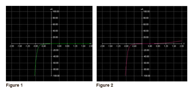
Figures 1 and 2 show I-V curves for two tested units (one passing and one failing). Units displaying shifts of more than 10% indicate failure at the tested voltage.