
ESD Solutions
High-speed
High-speed ESD Solutions: LVDS
Summary
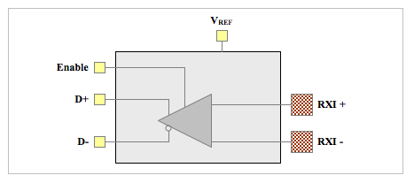
The LVDS I/O is a three-module design (input, output and reference block). Driver operates up to 1 GHz and receiver can operate up to 1.2 GHz (smaller technologies). The Driver is designed to drive either 50Ω or 100Ω differential termination. This cell has been designed to meet a set of the standard LVDS specifications (IEEE Std 1596.3-1996, Low Voltage Differential Signaling).
Diagram (input)

Key Features
- Powered from 1.8V ±10% and 1.0V (±10%) to 1.1V (-10%/+5%) core power supplies
- Operates up to 1.2GHz (2.4Gbps) (technology dependant)
- Input receive sensitivity of 75mV peak differential (without hysteresis)
- Common mode range from 0V to 2.4V (limited by Power Supply)
- Power-up sequence independent
- Low power consumption
- CML interface to core
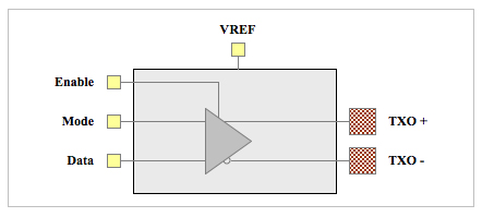
Diagram (driver)
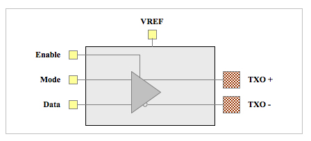
Features
- Powered from 1.8V ±10% and 1.0V to 1.1V (±10%) core power supplies
- Operates up to 1 GHz (2Gbps) with external 1 pF load (technology dependant)
- Common mode output range 1.22 Volts ±50mV
- Power-up Sequence Independent
- Low differential skew between TXO_P and TXO_N
- Mode control for output drive control to drive either 100Ω (3.25 mA) or 50Ω (6.50 mA) termination
- Low power consumption
Recommended Operating Conditions
| Symbol | Description | Min | Nom | Max | Units |
|---|---|---|---|---|---|
| VVDD | Core supply voltage | 0.9 | 1.0 to 1.1 | 1.115 | V |
| VDVDD | I/O supply voltage | 1.62 | 1.8 | 1.98 | V |
| VVREF | Reference voltage | 1.2 | V | ||
| TA | Ambient operating temperature | 0 | 25 | 100 | °C |
| TJ | Junction temperature | -40 | 25 | 125 | °C |
| VPAD | Voltage at PAD | -0.3V | VDVDD+0.3V | V |
Foundry Support
| Technology | Silicon proven / in production | Under development | Planned |
|---|---|---|---|
| 16nm | TSMC | ||
| 28nm | GF, TSMC | ||
| 40nm | GF, TSMC | ||
| 55nm | GF, TSMC | ||
| 65nm | GF, TSMC | ||
| 90nm | GF, TSMC | ||
| 110nm | |||
| 130nm | GF |
High-speed ESD Solutions: subLVDS
Summary
The LVDS I/O is a three-module design (input, output and reference block). Maximum operating frequency ranges from 250 MHz for 130 nm to 1GHz for 28nm. Driver cell is designed to drive either 50Ω or 100Ω differential termination. Meets the standard SubLVDS specifications (SMIA 1.0 Part 2:CCP2).
Receiver
Features
- Powered from 1.8V ±10% and 1.0V(±10%) to 1.1V(-10%/+5%) core power supplies
- Input receive sensitivity of 50mV peak differential (without hysteresis)
- Common mode range from 0.4V to 1.4V (limited by Power Supply)
- Power-up Sequence Independent
- Duty Cycle Distortion (DCD) less than 50ps
- Low power consumption
Driver
Features
- Powered from 1.8V ±10% and 1.0V to 1.1V (±10%) core power supplies
- Common mode output range 0.90 Volts +/-50mV
- Power-up Sequence Independent
- Differential Skew between TXO_P and TXO_N 50ps
- Mode control for output drive control to drive either 100Ω (1.5 mA typical) or 50Ω (3 mA typical) termination
- Low power consumption
Recommended Operating Conditions
| Symbol | Description | Min | Nom | Max | Units |
|---|---|---|---|---|---|
| VVDD | Core supply voltage | 0.9 | 1.0 to 1.1 | 1.115 | V |
| VDVDD | I/O supply voltage | 1.62 | 1.80 | 1.98 | V |
| VVREF | Reference voltage | 0.9 | V | ||
| TA | Ambient operating temperature | 0 | 25 | 100 | °C |
| TJ | Junction temperature | -40 | 25 | 125 | °C |
| VPAD | Voltage at PAD | -0.3V | VDVDD+0.3V | V |
Foundry Support
| Technology | Silicon proven / in production | Under development | Planned |
|---|---|---|---|
| 12nm | TSMC | ||
| 16nm | TSMC | ||
| 28nm | GF | ||
| 40nm | GF, TSMC | ||
| 55nm | GF | ||
| 65nm | GF | ||
| 90nm | |||
| 110nm | |||
| 130nm |