
ESD Solutions
Special
Special ESD Solutions: USB 1.1
Summary
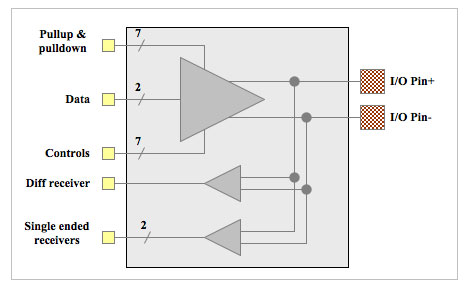
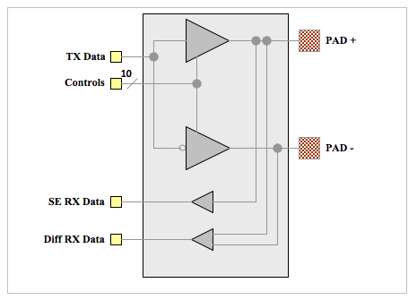
This library includes USC_BI_100_33V_SC cell is a dual mode (full-speed and low-speed) host capable Universal Serial Bus (USB 1.1 analog transceiver) bidirectional I/O cell as well as two adapter cells designed to align USC_BI_100_33V_SC bus structure with core-limited and pad-limited libraries.
This cell is a macro cell that contains its own isolated power supplies (DVDD and DVSS), but shares VDD and VSS with the rest of the padring.
Diagram
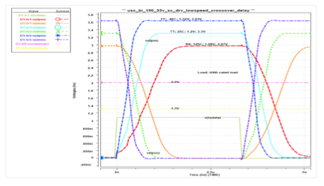
Simulation Results (low speed)
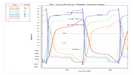
Simulation Results (full speed)
Foundry Support
| Technology | Silicon proven / in production | Under development | Planned |
|---|---|---|---|
| 28nm | GF | ||
| 40nm | |||
| 55nm | GF | ||
| 65nm | GF | ||
| 90nm | GF, TSMC | ||
| 110nm | |||
| 130nm | GF, TSMC |
Special ESD Solutions: ONFI
Summary
This ONFI I/O library includes the combo driver / receiver cells, the ODT / driver impedance calibration cell, and a full complement of power and support cells for both single-ended and differential ONFI 3.0 signaling.
Features
- Single-ended and differential ONFI signaling
- On-die termination
- Programmable drive strength
- ODT / driver output impedance calibration
- Operating frequency up to 200 MHz (400 MT/sec)
- Staggered I/O implementation
- Power-up sequencing independent design with Power-on Control
- Robust ESD Protection
- 2KV ESD Human Body Model (HBM)
- 200 V ESD Machine Model (MM)
- 500 V ESD Charge Device Model (CDM)
Diagram (driver)
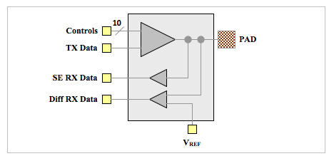
Diagram (clock driver)
Recommended Operating Conditions
| Parameter | Description | Min | Nom | Max | Units |
|---|---|---|---|---|---|
| VVDD | Core supply voltage | 0.99 | 1.1 | 1.21 | V |
| VDVDD | I/O supply voltage | 1.65 | 1.8 | 1.95 | V |
| TJ | Junction temperature | -40 | 25 | +125 | °C |
| VPAD | Voltage at PAD | VDVSS | VDVDD | V | |
| VIH | High-level input Voltage at IO | 0.7 * VDVDD | VDVDD + 0.3 | V | |
| VIL | Low-level input Voltage at IO | VDVSS – 0.3 | 0.3 * VDVDD | V |
Foundry Support
| Technology | Silicon proven / in production | Under development | Planned |
|---|---|---|---|
| 16nm | TSMC | ||
| 28nm | TSMC | GF | |
| 40nm | TSMC/GF | ||
| 55nm | |||
| 65nm | TSMC | ||
| 90nm | |||
| 110nm | |||
| 130nm |
Special ESD Solutions: Oscillators
Summary
Aragio Solutions offers several low jitter oscillator designs that can be used with a wide range of crystals.
32 KHz Oscillator
The OSx_BI_032_25V oscillator is designed to generate an asynchronous on-chip clock signal with an appropriate external oscillator crystal. The design has been optimized for low power, stability and minimum jitter using a general purpose 32KHz crystal. The design has been characterized to allow a variation of 4pF to 18pF on each pin.
Diagram
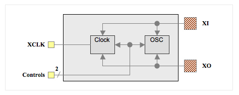
Key features
- Very low power (2.6 µW max)
- Bypass mode
- Power down (disable) mode
- Speed-up circuitry for fast startup
100 MHz Oscillator
The OSx_BI_100_25V oscillator is designed to generate an asynchronous on-chip clock signal with an appropriate external oscillator crystal. The design has been optimize for a wide operating range, stability and minimum jitter using a wide range of industry standard crystals. The design has been characterized to allow a variation of 4pF to 18pF on each pin.
Diagram
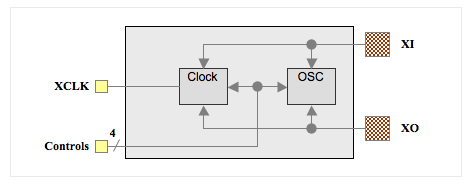
Key features
- Programmable current for wide frequency range
- Frequency range of 1 MHz to 100 MHz
- DVDD options from 1.5V to 2.5V
- Bypass mode
- Power down (disable) mode
- CML interface to core
Recommended Operating Conditions
| Description | Min | Nom | Max | Units | |
|---|---|---|---|---|---|
| VDVDD | I/O supply voltage | 1.35 | 1.5 | 3.63 | V |
| TA | Ambient operating temperature | 0 | 25 | 100 | °C |
| VVDD | Core supply voltage | 0.9 | 1.0 to 1.2 | 1.32 | V |
| TJ | Junction temperature | -40 | 25 | 125 | °C |
| VPAD | Voltage at PAD | 0 | - | VDVDD | V |
| VIH | Input logic high | 0.7 * VDVDD | VDVDD + 0.3 | V | |
| VIL | Input logic low | VDVSS – 0.3 | 0.3 * VDVDD | V |
Foundry Support
| Technology | Silicon proven / in production | Under development | Planned |
|---|---|---|---|
| 07nm | TSMC | ||
| 12nm | TSMC | ||
| 16nm | TSMC | ||
| 28nm | GF, TSMC | ||
| 40nm | GF, TSMC | ||
| 55nm | GF | ||
| 65nm | GF, TSMC | ||
| 90nm | GF | ||
| 110nm | GF | ||
| 130nm | GF | ||
| 180nm | GF |
Special ESD Solutions: MII / RMII
Summary
This library includes MIx_BI_004_5T_NC pad, designed to conform to the Reduced Media Independent Interface™ (RMII™) specification intended for use between Ethernet PHYs and Switch ASICs. Under IEEE 802.3u an MII comprised of 16 pins for data and control is defined. In devices incorporating many MACs or PHY interfaces such as switches, the number of pins can add significant cost as the port count increases. Typical switch products in the industry today offer 12 to 24 ports in a single device. At 6 pins per port and 1 pin per switch ASIC, the proposed RMII specification would save 119 pins plus the extra power and ground pins to support those additional pins for a 12 port switch ASIC.
The purpose of this interface is to provide a low cost alternative to the IEEE 802.3u MII. Architecturally, the RMII specification provides for an additional reconciliation layer on either side of the MII but can be implemented in the absence of an MII.
Features
- Capable of supporting 10 Mb/s and 100Mb/s data rates
- A single clock reference is sourced from MAC to PHY (or from an external source)
- It provides independent 2 bit wide (di-bit) transmit and receive data paths
- It uses TTL signal levels, compatible with common digital CMO ASIC processes
- Clock frequency of 50 MHz or less to minimize EMI and IC I/O requirements
- Pin count independent of port density of the PHY
- Single synchronous clocking
- Reduction of required control pins
Diagram
Output V-I Curve
Recommended Operating Conditions
| Symbol | Description | Min | Nom | Max | Units |
|---|---|---|---|---|---|
| VDVDD | I/O supply voltage | 2.97 | 3.30 | 3.63 | V |
| TA | Ambient operating temperature | 0 | 25 | 100 | °C |
| VVDD | Core supply voltage | 0.9 | 1.0 to 1.2 | 1.32 | V |
| TJ | Junction temperature | -40 | 25 | 125 | °C |
| VPAD | Voltage at PAD | 0 | VDVDD | V | |
| VIH | Input logic high | 2.0 | - | V | |
| VIL | Input logic low | - | 0.8 | V | |
| VOH | Output high | VDVDD – 0.4 | - | V | |
| VOL | Output low | - | 0.4 | V |
Foundry Support
| Technology | Silicon proven / in production | Under development | Planned |
|---|---|---|---|
| 28nm | |||
| 40nm | |||
| 55nm | GF | ||
| 65nm | GF | ||
| 90nm | |||
| 110nm | |||
| 130nm | GF |
Special ESD Solutions: GMII
Summary
This library includes MIP_BI_001_33V_NC pad, designed to conform to the Gigabit Media Independent Interface™ (GMII™) specification intended for use between Ethernet PHYs and Switch ASICs. Under IEEE 802.3-2005 a GMII comprised of 8 pins for data and control is defined.
Diagram

Simulation Results
Recommended Operating Conditions
| Symbol | Description | Min | Nom | Max | Units |
|---|---|---|---|---|---|
| VDVDD | I/O supply voltage | 2.97 | 3.30 | 3.63 | V |
| TA | Ambient operating temperature | 0 | 25 | 100 | °C |
| VVDD | Core supply voltage | 0.9 | 1.0 to 1.2 | 1.32 | V |
| TJ | Junction temperature | -40 | 25 | 125 | °C |
| VPAD | Voltage at PAD | 0 | - | VDVDD | V |
| VIH | Input logic high | 1.7 | - | - | V |
| VIL | Input logic low | - | - | 0.9 | V |
| VIL_AC | Input high voltage AC | 1.9 | - | - | V |
| VIH_AC | Input low voltage AC | - | - | 0.7 | V |
| VOH | Output high | 2.1 | - | 3.6 | V |
| VOL | Output low | 0 | - | 0.5 | V |
| F | Frequency | 125 – 100ppm | 125 + 100ppm | MHz |
Foundry Support
| Technology | Silicon proven / in production | Under development | Planned |
|---|---|---|---|
| 28nm | |||
| 40nm | |||
| 55nm | GF | ||
| 65nm | GF | ||
| 90nm | |||
| 110nm | |||
| 130nm | GF |
Special ESD Solutions: (r)GMII
Summary
This library includes MIP_BI_SDS_33V_NC pad, designed to conform to the Gigabit Media Independent Interface™ (GMII™) specification intended for use between Ethernet PHYs and Switch ASICs and Reduced Gigabit Media Independent Interface (RGMII) specified in HP RGMII ver 1.3, 12/10/2000. Under IEEE 802.3-2005 a GMII comprised of 8 pins for data and control is defined.
Diagram
Recommended Operating Conditions
| Description | Min | Nom | Max | Units | |
|---|---|---|---|---|---|
| VDVDD | I/O supply voltage (GMII mode) | 2.97 | 3.3 | 3.63 | V |
| VDVDD | I/O supply voltage (RGMII mode) | 2.25 | 2.5 | 2.75 | V |
| TA | Ambient operating temperature | 0 | 25 | 100 | °C |
| VVDD | Core supply voltage | 0.9 | 1.0-1.1 | 1.15 | V |
| TJ | Junction temperature | -40 | 25 | 125 | °C |
| VPAD | Voltage at PAD | 0 | - | VDVDD | V |
| VIH | Input logic high (RGMII) | 1.7 | - | - | V |
| VIL | Input logic low (RGMII) | - | - | 0.7 | V |
| VIH | Input logic high (GMII) | 1.7 | - | - | V |
| VIL | Input logic low (GMII) | - | - | 0.9 | V |
| VIL_AC | Input high voltage AC (GMII) | 1.9 | - | - | V |
| VIH_AC | Input low voltage AC (GMII) | - | - | 0.7 | V |
| VOH | Output logic high voltage (GMII) | 2.1 | - | 3.6 | V |
| VOL | Output logic low voltage (GMII) | 0 | - | 0.5 | V |
| VOH | Output logic high voltage (RGMII) | 2.0 | - | VDVDD+0.3 | V |
| VOL | Output logic low voltage (RGMII) | -0.3 | - | 0.4 | V |
| F | Frequency | 2.5[*] – 100ppm | 125 + 100ppm | MHz |
Foundry Support
| Technology | Silicon proven / in production | Under development | Planned |
|---|---|---|---|
| 16nm | TSMC | ||
| 28nm | GF, TSMC | ||
| 40nm | GF, TSMC | ||
| 55nm | |||
| 65nm | GF | ||
| 90nm | |||
| 110nm | |||
| 130nm |
Special ESD Solutions: PCI 3.0
Summary
These pads are compatible with PCI Local Bus Specification Revision 3.0 for 3.3V signaling. Cell can be used for both 33MHz and 66MHz operation.
Includes:
Without Schmitt Trigger
With Schmitt Trigger

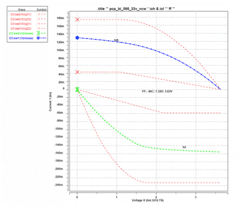
IOH/IOL (FF Corner)
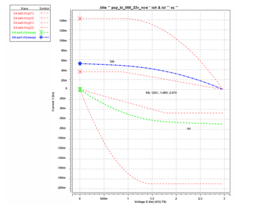
Special ESD Solutions: IOH / IOL (SS corner)
Recommended Operating Conditions
| Description | Min | Nom | Max | Units | |
|---|---|---|---|---|---|
| VDVDD | I/O supply voltage | 2.97 | 3.3 | 3.63 | V |
| TA | Ambient operating temperature | 0 | 25 | 100 | °C |
| VVDD | Core supply voltage | 0.9 | 1.1-1.2 | 1.26 | V |
| TJ | Junction temperature | -40 | 25 | 125 | °C |
| VPAD | Voltage at PAD | 0 | - | VDVDD | V |
| VIH | Input logic high | 0.7 * VDVDD | VDVDD + 0.3 | V | |
| VIL | Input logic low | VDVSS – 0.3 | 0.3 * VDVDD | V |
Foundry Support
| Technology | Silicon proven / in production | Under development | Planned |
|---|---|---|---|
| 28nm | GF | ||
| 40nm | GF | ||
| 55nm | GF | ||
| 65nm | GF | ||
| 90nm | |||
| 110nm | GF | ||
| 130nm | GF |