
ESD Solutions
Memory Interfaces
Aragio Solutions offers I/O pads for a wide range of memory interfaces:
DDR – SSTL_2
DDR2 – SSTL_18
DDR3 – SSTL_15
DDR2/DDR3 combo
LPDDR2
7 way DDR combo
Memory Interfaces: DDR – SSTL_2
Summary
The SSTL_2 pad set is a full complement of I/O, power, and spacer cells (total of 14 cells) that are necessary to assemble a padring by abutment. Since the SSTL_2 normally operates with its own isolated power domain (2.5V), a “rail-splitter” support cell (SPP_RS_005_25V) is included to allow the designer to easily break the lines that should not connect to the rest of the padring, while allowing VDD and VSS to be continuous within the padring.
The cells are designed to provide the user with the option of either Class I or Class II operation that is fully compliant with the JEDEC standard JESD8-9B specification (250 MHz maximum frequency).
The reason for providing a pad set is because special control signals (POC, VREF) that are unique to the SSTL_2 I/O pads are routed through the padring. Therefore, the spacer and power supply pads must have these unique signals routed through. The VREF signal is placed to minimize any noise coupling. This enables the VREF pad (SLP_RE_000_25V) to support up to 40 SSTL_2 drivers or clock pads.
Features
- JEDEC standard compliant
- Supports both Class I and Class II
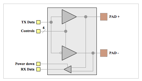
Diagram (driver)
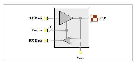
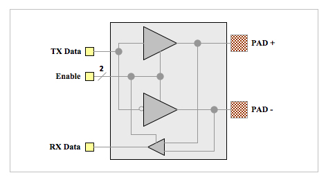
Diagram (clock driver)
Recommended Operating Conditions
| Parameter | Description | Min | Nom | Max | Units |
|---|---|---|---|---|---|
| VVDD | Core supply voltage | 0.90 | 1.0 to 1.2 | 1.32 | V |
| VDVDD | I/O supply voltage | 2.25 | 2.5 | 2.75 | V |
| VVREF | Reference voltage | 1.125 | 1.25 | 1.375 | V |
| TA | Ambient operating temperature | 0 | 25 | 100 | °C |
| TJ | Junction temperature | -40 | 25 | 125 | °C |
| VPAD | Voltage at PAD | 0 | VDVDD | V | |
| VIH (dc) | DC input logic high | VREF+125 | VDVDD+300 | mV | |
| VIL (dc) | DC input logic low | -300 | VREF-125 | mV | |
| VIH (ac) | AC input logic high | VREF+250 | - | mV | |
| VIL (ac) | AC input logic low | - | VREF-250 | mV |
Foundry Support
| Technology | Silicon proven / in production | Under development | Planned |
|---|---|---|---|
| 28nm | |||
| 40nm | TSMC | ||
| 55nm | GF, UMC | ||
| 65nm | GF | ||
| 90nm | GF | ||
| 110nm | |||
| 130nm | GF |
Memory Interfaces: DDR2 – SSTL_18
Summary
The SSTL_18 pad set is a full complement of I/O, power, and spacer cells that are necessary to assemble a padring by abutment. Since the SSTL_18 normally operates with its own isolated power domain (1.8V), a “rail-splitter” support cell is included to allow the designer to easily break the lines that should not connect to the rest of the padring, while allowing VDD and VSS to be continuous within the padring.
The output circuitry is designed with 2.5-volt FET’s, but all parameters are guaranteed only at 1.8 volts (±10%).
The cells are designed to provide the user with the option of either 60% or full drive that is fully compliant with the JEDEC standard JESD8-15a specification up to 400 MHz (DDR800) with balanced load management.
Features
- JEDEC standard compliant
- SSTL_18 with selectable 60% or full drive
- 2.5V FETs
- Up to 400 MHz with balanced load management
- Full complement of pads
- 50Ω, 75Ω and 150Ω termination
- Non-ODT reduced size driver and clock pad (30μm pitch)
Diagram (driver)
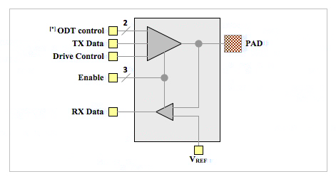
Diagram (clock driver)
Recommended Operating Conditions
| Parameter | Description | Min | Nom | Max | Units |
|---|---|---|---|---|---|
| VVDD | Core supply voltage | 0.90 | 1.0 to 1.2 | 1.32 | V |
| VDVDD | I/O supply voltage | 1.62 | 1.8 | 1.98 | V |
| VVREF | Reference voltage | 0.81 | 0.9 | 0.99 | V |
| TA | Ambient operating temperature | 0 | 25 | 100 | °C |
| TJ | Junction temperature | -40 | 25 | 125 | °C |
| VPAD | Voltage at PAD | 0 | VDVDD | V | |
| VIH (dc) | DC input logic high 1 | VREF+125 | VDVDD+300 | mV | |
| VIL (dc) | DC input logic low 1 | -300 | VREF-125 | mV | |
| VIH (ac) | AC input logic high 1 | VREF+250 | - | mV | |
| VIL (ac) | AC input logic low 1 | - | VREF-250 | mV |
Foundry Support
| Technology | Silicon proven / in production | Under development | Planned |
|---|---|---|---|
| 28nm | |||
| 40nm | TSMC | ||
| 55nm | GF | ||
| 65nm | GF, TSMC | ||
| 90nm | GF | ||
| 110nm | |||
| 130nm | GF |
Memory Interfaces: DDR3 – SSTL_15
Summary
The SSTL_15 pad set is a full complement of I/O, calibration, power, and spacer cells that are necessary to assemble a padring by abutment. Since the SSTL_15 normally operates with its own isolated power domain (1.5V), a “rail-splitter” support cell (SPP_RS_005_15V) is included to allow the designer to easily break the lines that should not connect to the rest of the padring, while allowing VDD and VSS to be continuous within the padring.
Features
- Full DDR3 capability – 800MHz (1600 Mbps)
- Low Power driving standard DDR3 memories
- 1.8V FETs
- Full complement of cells to build padring (20)
- Full ODT Capability:
- Either fixed 6-Bit programmation (program from core)
- Or, dynamic 6-Bit PVT calibration (external reference resistor)
Diagram (driver)
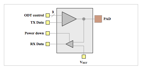
Diagram (clock driver)
Recommended Operating Conditions
| Parameter | Description | Min | Nom | Max | Units |
|---|---|---|---|---|---|
| VVDD | Core supply voltage | 0.9 | 1.0 to 1.1 | 1.115 | V |
| VDVDD | I/O supply voltage | 1.425 | 1.5 | 1.575 | V |
| VVREF | Reference voltage | 0.49*DVDD | DVDD /2 | 0.51*DVDD | V |
| TA | Ambient operating temperature | 0 | 25 | 100 | °C |
| TJ | Junction temperature | -40 | 25 | 125 | °C |
| VPAD | Voltage at PAD | 0 | VDVDD | V | |
| VIH (dc) | DC input logic high | VREF + 0.1 | V | ||
| VIL (dc) | DC input logic low | VREF – 0.1 | V | ||
| VIH (ac) | AC input logic high | VREF + 0.175 | - | V | |
| VIL (ac) | AC input logic low | - | VREF – 0.175 | V |
Foundry Support
| Technology | Silicon proven / in production | Under development | Planned |
|---|---|---|---|
| 28nm | GF | TSMC | |
| 40nm | GF, TSMC | ||
| 55nm | |||
| 65nm | GF, TSMC | ||
| 90nm | |||
| 110nm | |||
| 130nm |
Memory Interfaces: DDR2 / DDR3 Combo
Summary
The SSTL_15/18 pad set is a full complement of I/O, calibration, power, and spacer cells that are necessary to assemble a padring by abutment. Since the SSTL_15/18 normally operates with its own isolated power domain (1.5V/1.8V), a “rail-splitter” support cell (SPP_RS_005_15V) is included to allow the designer to easily break the lines that should not connect to the rest of the padring, while allowing VDD and VSS to be continuous within the padring.
Features
- Full DDR3 capability – 800MHz (1600 Mbps)
- Full DDR2 capability
- Low Power driving standard DDR3 memories
- Full complement of cells to build padring (20)
- Full ODT Capability – dynamic 6-Bit PVT calibration (external reference resistor)
Diagram (driver)
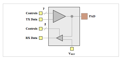
Diagram (clock driver)
Recommended Operating Conditions
| Parameter | Description | Min | Nom | Max | Units |
|---|---|---|---|---|---|
| VVDD | Core supply voltage | 0.9 | 1.1 to 1.2 | 1.26 | V |
| VDVDD (SSTL_15) | I/O supply voltage | 1.425 | 1.5 | 1.575 | V |
| VDVDD (SSTL_18) | I/O supply voltage | 1.62 | 1.8 | 1.98 | V |
| VVREF | Reference voltage | 0.81 | 0.9 | 0.99 | V |
| TA | Ambient operating temperature | 0 | 25 | 100 | °C |
| TJ | Junction temperature | -40 | 25 | 125 | °C |
| VPAD | Voltage at PAD | 0 | VDVDD | V | |
| VIH (dc) | DC input logic high | VREF + 0.1 | V | ||
| VIL (dc) | DC input logic low | TBD | VREF – 0.1 | V | |
| VIH (ac) | AC input logic high | VREF + 0.175 | - | V | |
| VIL (ac) | AC input logic low | - | VREF – 0.175 | V |
Foundry Support
| Technology | Silicon proven / in production | Under development | Planned |
|---|---|---|---|
| 28nm | GF, TSMC | ||
| 40nm | GF, TSMC | ||
| 55nm | |||
| 65nm | GF | TSMC | |
| 90nm | |||
| 110nm | |||
| 130nm |
Memory Interfaces: LPDDR2
Summary
- Includes a full complement of pads to assemble a LPDDR2 padring:LPDDR2 driver / receiver
- LPDDR2 driver / receiver with CKE held low at power ramp
- Differential clock cell
- Power/ground pads
- spacers
Diagram (driver)
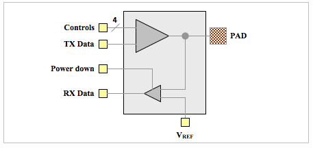
Diagram (clock)
Recommended Operating Conditions
| Parameter | Description | Min | Nom | Max | Units |
|---|---|---|---|---|---|
| VDVDD | mDDR supply voltage | 1.14 | 1.2 | 1.3 | V |
| VVDD | Core supply voltage | 0.8 | 1.0-1.2 | 1.32 | V |
| TJ | Junction temperature | -40 | 25 | 125 | °C |
Foundry Support
| Technology | Silicon proven / in production | Under development | Planned |
|---|---|---|---|
| 28nm | GF | ||
| 40nm | |||
| 55nm | GF | ||
| 65nm | GF | ||
| 90nm | |||
| 110nm | |||
| 130nm |
Memory Interfaces: 7 way DDR combo
Summary
The LPDDR2/3_DDR3/4 libraries contain the 7-way combo driver/receiver cells with embedded power cells, the driver impedance calibration cell, and the DDR voltage reference cell providing both single-ended and differential signaling for LPDDR2, LPDDR3, LPDDR4, DDR3, DDR3L, DDR3U, and DDR4 applications. Also included is a full complement of power, corner and spacer cells to assemble a complete pad ring by abutment. An included rail splitter allows multiple power domains to be isolated in the same pad ring while maintaining continuous VDD/VSS for robust ESD protection.
Features
- Full DDR4 capability
- Data rates – 1600 MT/s, 1866 MT/s, 2133 MT/s, 2400 MT/s
- Full DDR3 / DDR3L / DDR3U capability
- Data rates – 800 MT/s, 1066 MT/s, 1333 MT/s, 1600 MT/s, 1866 MT/s, 2133 MT/s
- Full LPDDR4 capability
- Data rates – 1066 MT/sec, 2400 MT/sec, 3200 MT/sec, 4266 MT/sec
- Full LPDDR3 capability
- Data rates – 1333 MT/sec, 1600 MT/sec
- Full LPDDR2 capability
- Data rates – 466 MT/sec, 1066 MT/sec
- User programmable drive strength
- DDR3 – ZOUT = 34 / 40 Ω
- DDR4 – ZOUT = 34 / 48 Ω
- LPDDR2 – ZOUT = 34 / 40 / 48 / 60 / 80 Ω
- LPDDR3 – ZOUT = 34 / 40 Ω
- LPDDR4 – ZOUT = 40 / 48 / 60 / 80 / 120 / 240 Ω
- User programmable on-die termination
- DDR3 – 120 / 60 / 40 / 30 / 24 / 20 / 17 Ω
- DDR4 – 240 / 120 / 80 / 60 / 48 / 40 / 34 Ω
- LPDDR3 – 240 / 120 / 80 / 60 / 48 / 40 / 34 Ω
- LPDDR4 – 240 / 120 / 80 / 60 / 48 / 40 / 34 Ω
Diagram (driver)
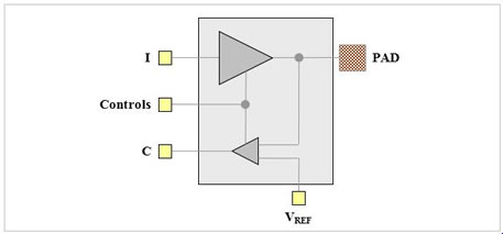
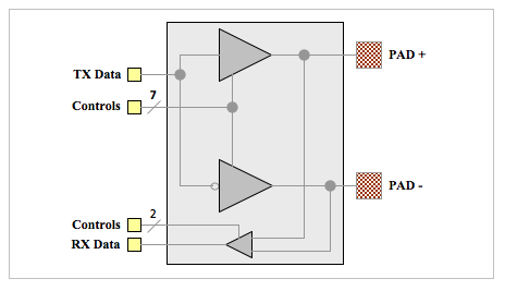
Diagram (clock)

Recommended operating conditions
| Parameter | Description | Min | Nom | Max | Units | |
|---|---|---|---|---|---|---|
| VVDD | Core supply voltage | 0.72 | 0.80 | 0.88 | V | |
| VDVDD | I/O supply voltage | DDR4 | 1.14 | 1.2 | 1.26 | V |
| DDR3 | 1.425 | 1.5 | 1.575 | V | ||
| DDR3L | 1.283 | 1.35 | 1.45 | V | ||
| DDR3U | 1.19 | 1.25 | 1.31 | V | ||
| LPDDR2 | 1.14 | 1.2 | 1.3 | V | ||
| LPDDR3 | 1.14 | 1.2 | 1.3 | V | ||
| LPDDR4 | 1.06 | 1.1 | 1.17 | V | ||
| TJ | Junction temperature | -40 | 25 | +125 | °C | |
| VPAD | Voltage at PAD | VDVSS |
|
VDVDD | V | |
| Technology | Silicon proven / in production | Under development | Planned |
|---|---|---|---|
| 12nm | TSMC | ||
| 16nm | TSMC | ||
| 28nm | TSMC | ||
| 40nm | TSMC |